Scattering Waves
By Geno Cathy IV
Yagi-Uda Patch Antenna Array
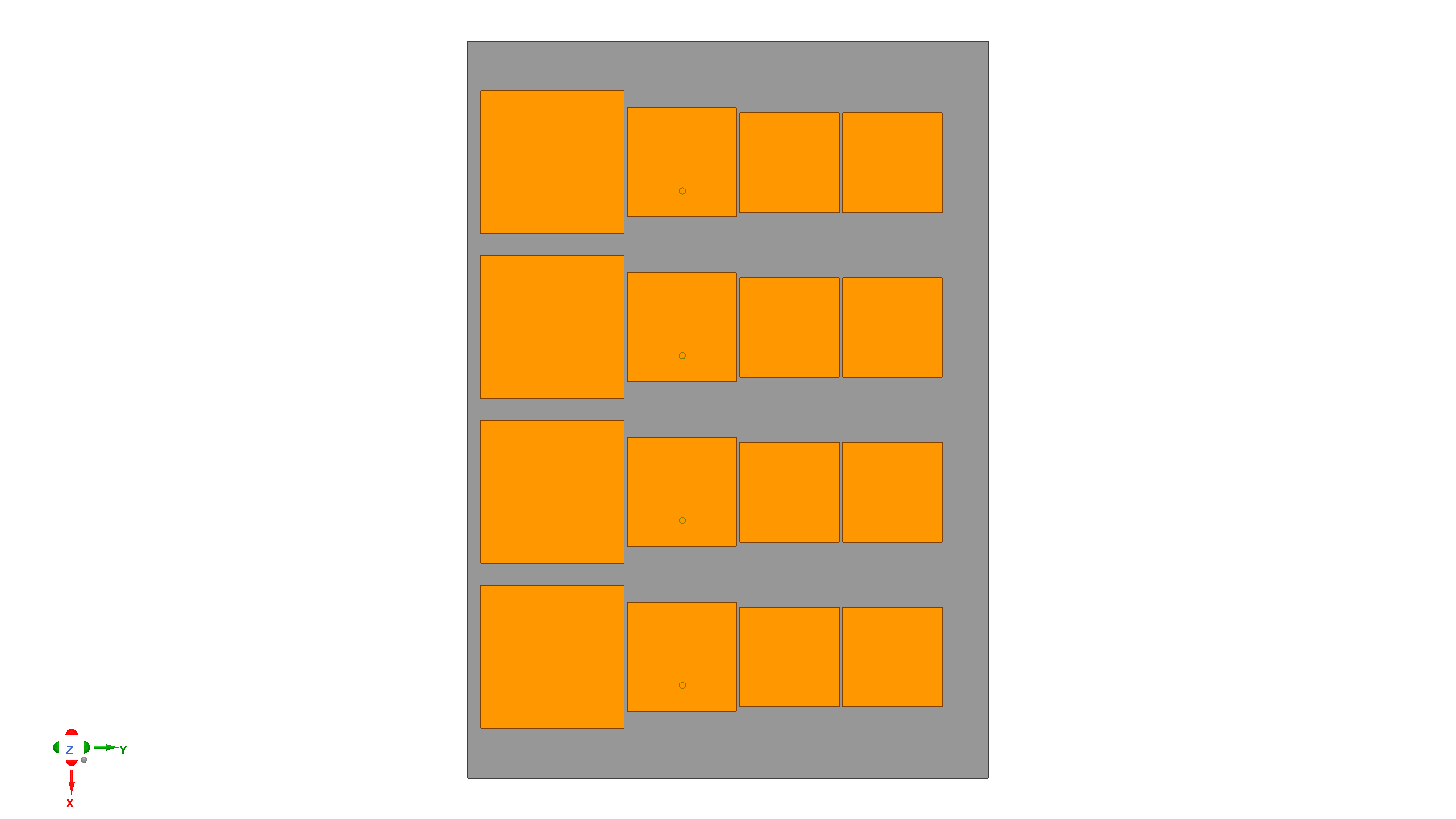
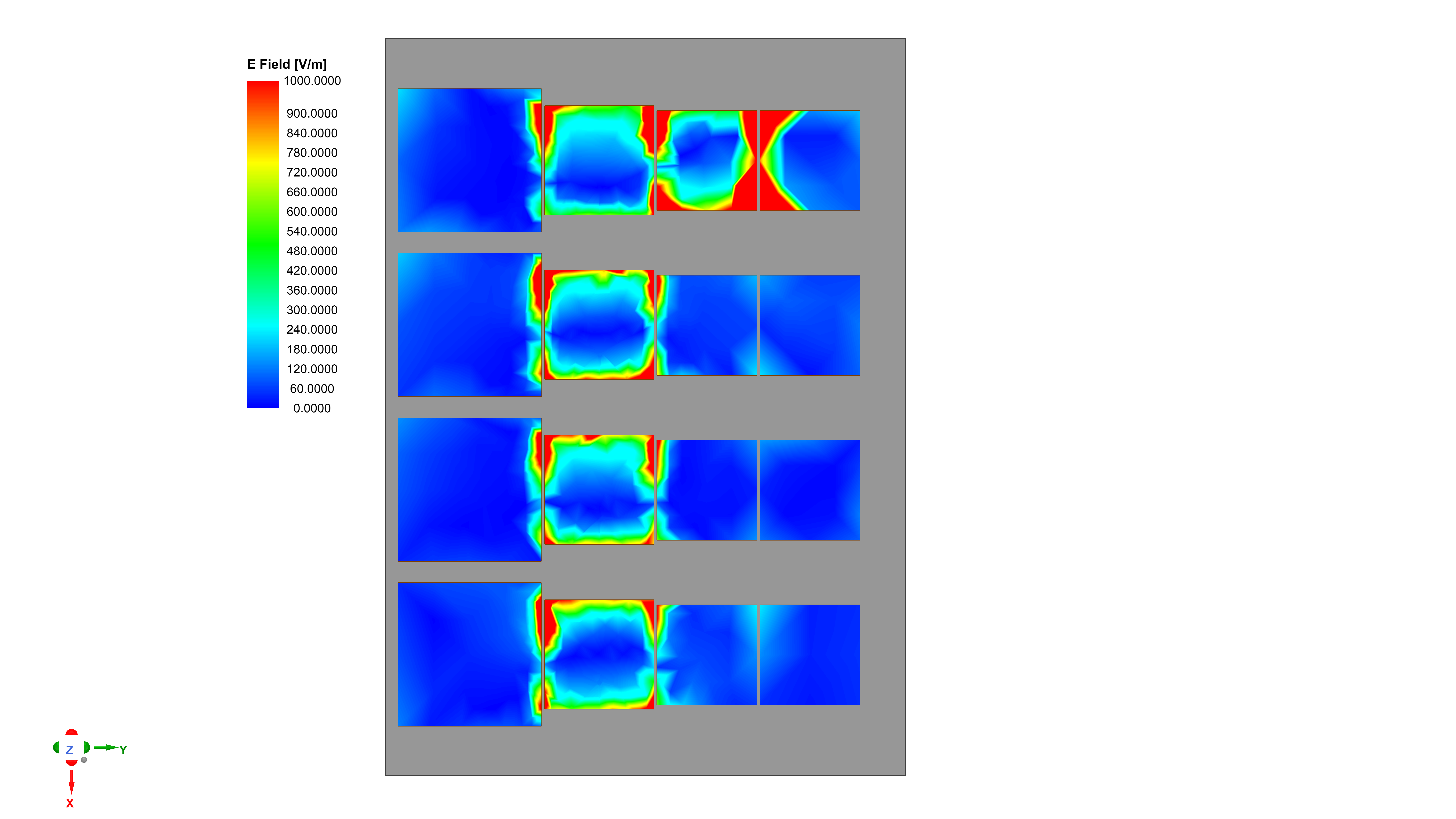
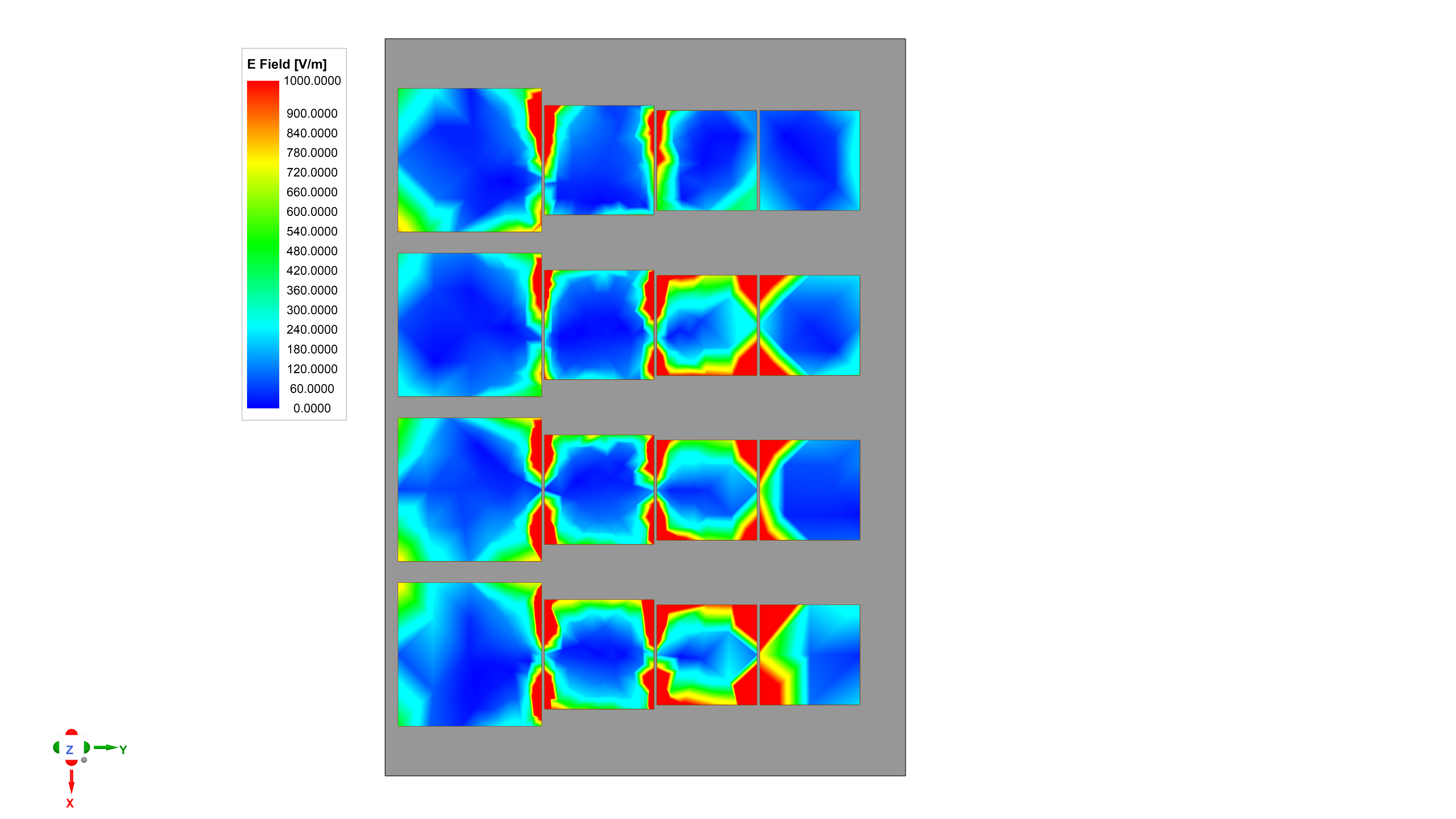
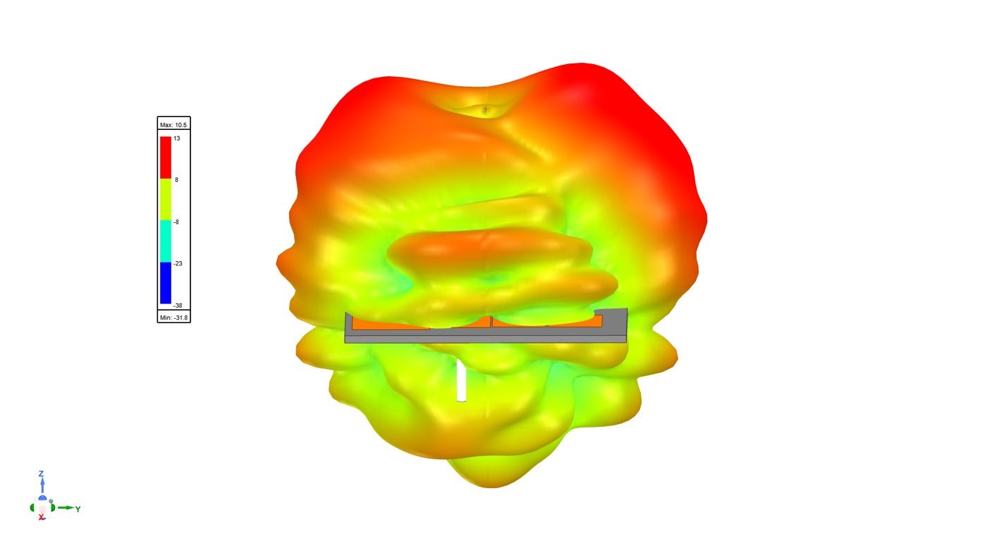
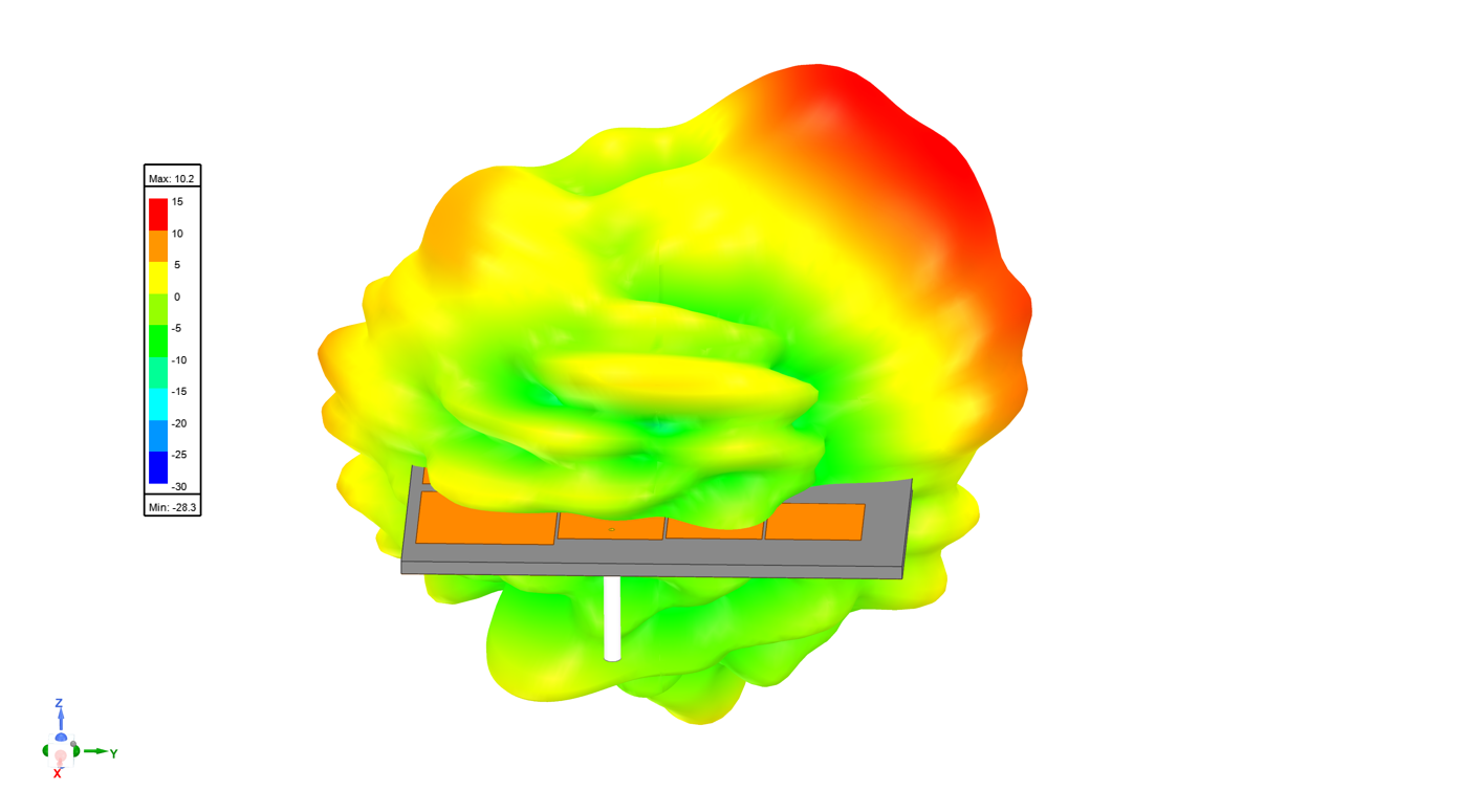
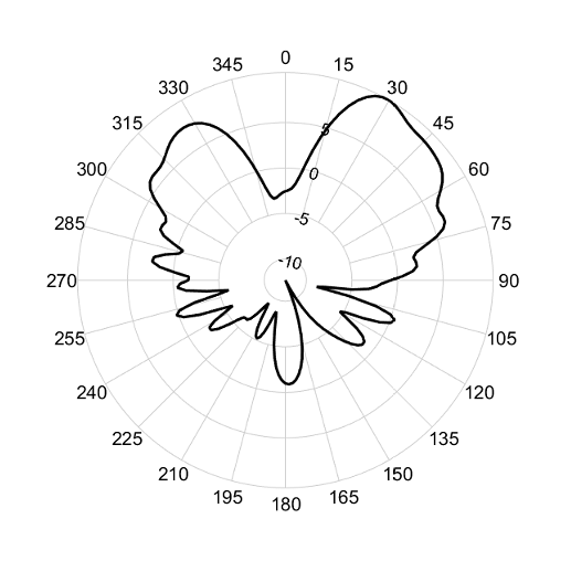
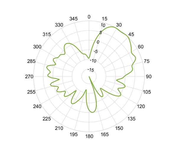
The Yagi-Uda microstrip patch antenna array designed in HFSS can be seen in Fig. 2. Which consists of sixteen elements, with four reflectors, four driven elements, and eight directors. The design models the Yagi-Uda array consisting of linear dipole elements, but instead of dipoles they are square patches. The electromagnetic energy is not only transferred from space but also through surface waves. Surface waves are caused by the conducting element and the dielectric substrate [4]. Furthermore, microstrip patch antennas predominately radiated in the broadside direction, therefore mutual coupling between other patches on the substrate are inefficient. As a result, to make the microstrip patch Yagi-Uda antenna array effective for mutual coupling, spacing for each adjacent reflector and director must be nearly-touching. The spacing for the reflector is the main contributor in the design and should not have spacing more than 0.3λ or the gain can drop significantly [1]. When designing the Yagi-Uda patch antenna array, [3] was used to get preliminary empirical data points for spacing and sizing of elements. The original design operated in the L-band and had an unusually large substrate thickness of 6.35 mm. Subsequently, as an alternative, the Yagi-Uda patch antenna array was designed to operate in the C-band with a much more practical substrate thickness of 1.575 mm. The substrate used for the C-band design is a Rogers RT5880 with a relative permittivity of 2.2 and a loss tangent of 0.0009.The spacing between the reflector and driven element are 1.9658 mm apart. Additionally, the driven element and the first director have a spacing of 0.587 mm, while the spacing is 0.381 mm for the first director to the second director. As it can be realized, the gap distances are fairly close which provides a salient point that surface waves are a primary effectn when shifting the radiation pattern from broad side. It can then be assumed that the dielectric thickness and the relative permittivity along with the dimensions of the substrate play a role in the make up of the surface waves. In addition,these distances were found by empirical simulation results. These gaps were found to have the greatest impact on shifting the radiation pattern to end-fire. Further, another important factor for shifting the radiation to end-fire was the length and width dimensions of the entire substrate. Again, this was found empirically by running multiple iterations in HFSS to find the greatest impact in shifting the radiation pattern. The optimal dimension for the substrate is 60 mm x 85 mm. These dimensions are significantly smaller than [3], granted the resonant frequency was much lower. However, the size of [3] seems to be much larger than necessary due to the spacing of each row. Supplementary, the spacing for each row entertains another factor in how the radiation pattern along with the realized gain is effected. From empirical simulation results the spacing for each row was found to be 2.49 mm. If the spacing between each row was too far from each other the gain would drastically decreases along with the elevation tilt away from broadside. Lastly, the pin location for the driven element needs to be considered as the location affects the radiation pattern and the input reflection coefficient of the antenna.