8 GHz Single-Stage Microwave Transistor Amplifier
In this report, an 8 GHz single-stage microwave transistor amplifier is designed and fabricated. By utilizing conjugate matching using open stubs the single-stage microwave transistor amplifier is designed to have a theoretical gain of 17.5 dB
using a BFU710 NPN wide band silicon germanium (SiGe) RF transistor. The single-stage microwave transistor amplifier consists of a Rogers RT6002 substrate that has a dielectric thickness of 1.52 mm and a copper thickness value of 35 µm. Further, the measured single-stage
microwave transistor amplifier had a maximum gain (\(|S_{21}|\)) of 12.42 dB, while having an input reflection coefficient (\(|S_{11}|\)) value of -13.52 dB at a resonant frequency of 7.625 GHz. The frequency of operation of the measured results shifted by 0.375 GHz. Additionally, the
design procedures and matching results will be discussed.
It’s important to discuss the foundation of how electromagnetic waves transmit and reflect in a two-port network. In the schematic below, a general two-port network with a source andload impedance is considered.
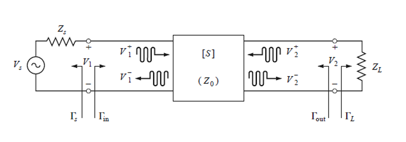
Where the scattering matrix is characterized as the two-port network. \(\Gamma = \frac{Z_L-Z_0}{Z_L+Z_0}\) and \(\Gamma = \frac{Z_S-Z_0}{Z_S+Z_0}\) shows the reflection coefficient looking towards the load and the reflection coefficient looking towards the source, respectively.
Furthermore, to successfully design a single-stage microwave transistor amplifier \(\Gamma_{in}$\) and \(\Gamma_{out}\) need to be purposefully mismatched. Therefore, (1) and (2) can be quickly deduced as:
\(\Gamma_{in} = \frac{V^-_1}{V^+_1} = S_{11} + \frac{S_{12}S_{21}\Gamma_L}{1-S_{22}\Gamma_L}\) (1)
\(\Gamma_{out} = \frac{V^-_2}{V^+_2} = S_{22} + \frac{S_{12}S_{21}\Gamma_s}{1-S_{11}\Gamma_s}\) (2)
Thus, to design a single-stage microwave transistor amplifier for maximum gain, conjugate matching needs to be utilized where:
\(\Gamma_{in} = \Gamma^{\ast}_S\) (3)
\(\Gamma_{out} = \Gamma^{\ast}_L\) (4)
The circuit below, shows a model of an input matching circuit, transistor characterized by its respective scattering parameters, and the output matching circuit. Where \(G_s\) is equal to the input matching, \(G_0\) is equal to the transistor, and \(G_L\) is equal to the output matching. As a result, the gain for each section can be calculated.
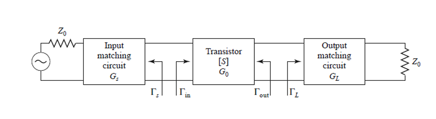
Thus, it is advantageous to find the total gain of the RF transistor along with its respective input and output matching circuits before continuing with a specific RF transistor. Each gain equation can be seen in (5), (6), and (7).
\(G_S = \frac{1-|\Gamma_s|^2}{|1-\Gamma_{in}\Gamma_S|^2}\) (5)
\(G_0 = |S_{21}|^2\) (6)
\(G_L = \frac{1-|\Gamma_L|^2}{|1-S_{22}\Gamma_L|^2}\) (7)
If the RF transistor is unilateral, meaning \(S_{12}\) is equal to zero, then the unilateral gain can be calculated by (8).
\(G_{TU} = G_sG_0G_L\) (8)
By using these equations, it will be easier to narrow down the selection of single-stage microwave transistor amplifier for specific applications or requirements. Furthermore, Stability of an single-stage microwave transistor amplifier is a crucial parameter to consider. If the input or output ports have a negative real part
that implies that oscillation has occurred [1]. There are two types of stability equations and they can be classified by using either the K-\(\Delta\) test or the \(\mu\) test. In this paper the K-\(\Delta\) is utilized. Further, the network is classified as unconditionally stable when K > 1, and \(|\Delta|\) < 1. (9) and (10) show both test conditions.
\(K = \frac{1-|S_{11}|^2-|S_{22}|^2+|\Delta|^2}{2|S_{12}S_{21}|}\) (9)
\(|\Delta| = |S_{11}S_{21}-S_{12}S_{21}|\) (10)
If only one of these conditions are met, the network is said to be potentially unstable. Further, stability conditions are usually frequency dependent since the matching network is dependent on frequency [1]. Now, if the K - \(\Delta\) condition is not satisfied, stability circles will need to be created via the Smith chart. The centers and radiis for the
source side and load side can be calculated by using (11), (12), (13), and (14), respectively.
\(C_S = \frac{(S_{11}-\Delta S^{\ast}_{22})^{\ast}}{|S_{11}|^2-|\Delta|^2}\) (11)
\(R_S = \frac{|S_{12}S_{21}|}{|S_{11}|^2-|\Delta|^2}\) (12)
\(C_L = \frac{(S_{22}-\Delta S^{\ast}_{11})^{\ast}}{|S_{22}|^2-|\Delta|^2}\) (13)
\(R_L = \frac{|S_{12}S_{21}|}{|S_{22}|^2-|\Delta|^2}\) (14)
When these values are calculated and plotted on a Smith chart unstable regions of the input and output will be realized. Moreover, Once the RF transistor has been verified that it is unconditionally stable at the frequency of operation by means of the K-\(\Delta\) test, the matching circuits can be designed. Following the criteria from (5) and (6), provide
these two equation for plotting on the Smith chart:
\(\Gamma_S = \frac{B_1\pm\sqrt{B^2_1-4|C_1|^2}}{2C_1}\) (15)
\(\Gamma_L = \frac{B_2\pm\sqrt{B^2_2-4|C_2|^2}}{2C_2}\) (16)
Then the variables are defined by:
\(B_1 = 1+|S_{11}|^2-|S_{22}|^2-|\Delta|^2\) (17)
\(B_2 = 1+|S_{22}|^2-|S_{11}|^2-|\Delta|^2\) (18)
\(C_1 = S_{11}-\Delta S^{\ast}_{22}\) (19)
\(C_2 = S_{22}-\Delta S^{\ast}_{11}\) (20)
Once these equations are calculated \(\Gamma_S\) and \(\Gamma_L\) can be plotted on the Smith chart. The matching done on the Smith chart for the 8 GHz single-stage microwave transistor amplifier consisted of open stub matching. Once the matching circuits are found, ADS is utilized to design the circuit. The figure below, shows the the baseline design with ideal components.
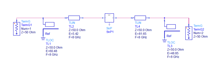
The design consists of ideal open circuited stubs, ideal transmission lines, and a .s2p file which includes the RF transistors scattering parameters at 8 GHz. The dielectric substrate used is a Rogers RT6002 with a thickness of 1.52 mm and a copper thickness of 1 oz or 35\(\mu m\). The relative permittivity is 2.94, and the dissipation factor is 0.0012 at 10 GHz. Further,
the baseline designed is first constructed with ideal components to verify that the calculated values matched the simulation results. Once calculations matched the simulation results, non ideal components are simulated. To use non ideal components microstrip equations are used in order to calculate the appropriate widths and lengths of the transmission lines and open
circuited stubs. To calculate the width of the microstrip line and open circuited stubs, (21) and (22) may be used. To use (21) and (22) the characteristic impedance (\(Z_0\)) and relative permittivity (\(\epsilon_r\)) must be known. Then an initial guess must be realized. If \(\frac{W}{d} \leq 1\) then (21) must be used. If the initial guess is incorrect and the ratio of
\(\frac{W}{d}\) is larger. Then (22) must be used.
\(\frac{W}{d} = \frac{8e^A}{e^{2A}-2}\) (21)
\(\frac{2}{\pi}[B-1-ln(2B-1)+\frac{\epsilon_r-1}{2\epsilon_r}\{ln(B-1)+0.39-\frac{0.61}{\epsilon_r}\}] \) (22)
Then to calculate the A or B variable (23) and (24) can be realized, respectively.
\(A = \frac{Z_0}{60}\sqrt{\frac{\epsilon_r+1}{2}}+\frac{\epsilon_r-1}{\epsilon_r+1}(0.23+\frac{0.11}{\epsilon_r})\) (23)ee
\(B = \frac{377\pi}{2Z_0\sqrt{\epsilon_r}}\) (24)
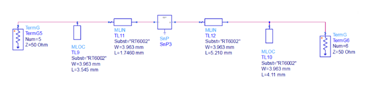
Additionally, to speed up the calculations a program in ADS called LineCalc is used to calculate the microstrip widths. Once the microstrip lengths and widths are calculated, non ideal microstrip lines and microstrip open circuited stubs are implemented, which can be seen below. The width for each microstrip line and open circuited stub is 3.963 mm. Likewise, the lengths all
had different values due to the calculations for the matching networks.
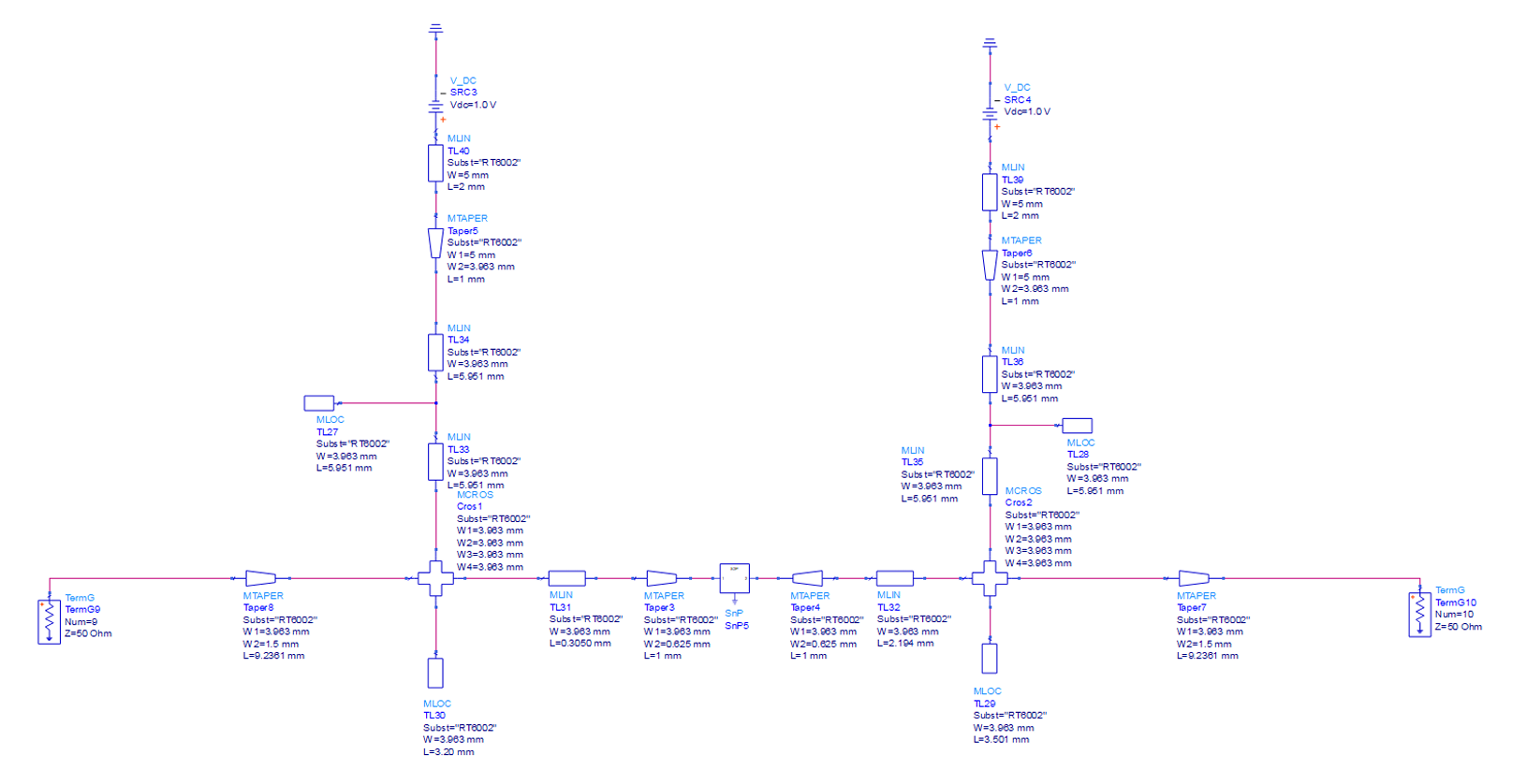
Furthermore, after the non ideal circuit simulation matched the calculated gain, a DC bias network along with tapering is added to the circuit schematic for the microwave transistor. When the additional microstrip lines for tapering are added, the microstrip lines along with the open circuited stubs of the matching circuits needed to be tuned so that the resonant frequency along with
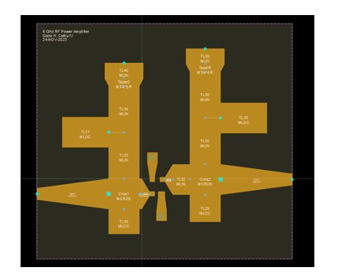
the gain stayed at the frequency and gain of interest. The final circuit and layout with the DC biasing and tapering can be seen below, respectively.
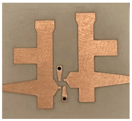
The fabricated 8 GHz single-stage microwave transistor amplifier can be viewed below:
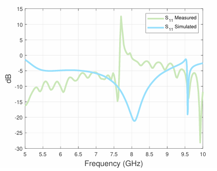
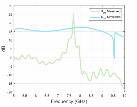
Moreover, The figure below show the gain and input reflection coefficient across frequency, respectively. Each figure shows the simulated versus measured results. As it can be viewed, the gain in the simulation results from ADS show good agreement with the theoretically calculated gain. The simulated gain at 8 GHz is 17.405 dB, while a gain of 17.5 dB was realized by theoretical calculations.
Comparatively, the measured results show a gain of 12.424 dB at 7.625 GHz. The frequency shifts 0.375 GHz down from the frequency of interest. The shift in frequency can be accounted for due to the thickness of the simulated dielectric substrate versus the fabricated dielectric substrate. Due to the milling process, some of the dielectric substrate thickness was removed. Therefore, decreasing the overall
thickness of the dielectric substrate. Thus shifting the resonant frequency. Additionally, the measured results show that as the frequency increases, the single-stage microwave transistor amplifier starts to behave like an oscillator. The figure below shows the input reflection coefficient across frequency for both simulated and measured results.
At 8 GHz the simulated results show an input reflection coefficient of -19.734 dB, while the measured results show an input reflection coefficient of -13.523 dB at 7.625 GHz. It can be clearly depicted in this figure that the single-stage microwave transistor amplifier starts to have characteristics of an oscillator. The alarming spike in regard to the input reflection coefficient in the figure above, shows
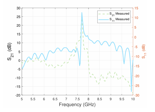
that the wave is propagating through the transistor getting amplified and then being reflected from the load right back to the source. The plot below, shows a plot of both the measured \(S_{11}\) and \(S_{21}\) scattering parameters. As it can be viewed as the frequency increases past 7.625 GHz the gain increases to a maximum of 25.118 dB at 7.70 GHz, while having an input reflection coefficient of 12.757 dB.
An 8 GHz single-stage microwave transistor amplifier was designed for maximum gain by means of conjugate matching. The input and output matching consisted of open circuited stubs with a transmission feed line at a certain distance from the load. Further, simulation results have good agreement with the theoretical calculations for gain, while the measured versus simulation results show similar characteristics.
The overall gain of the measured single-stage microwave transistor amplifier is 12.424 dB, while having an input reflection coefficient of -13.523 dB at 7.625 GHz. The process of etching out the copper from the dielectric substrate can account for the frequency shifted and loss of gain. Likewise, the oscillation behavior at 7.625 GHz may also be due the loss of dielectric substrate thickness, however, due to time
constraints a further study could not be made.
[1] D. M. Pozar, Microwave Engineering, 4thed. Hoboken, NewJersey :John Wiley and Sons,2012.